This article is from wechat public number: Guojun Industry Research (ID: industryRCofG), author: Xiao Jie, Bao Yanxin, original title: "Advanced packaging industry chain depth report (2) - Packaging substrate materials contain development opportunities, leading enterprises show growth potential", caption from: Vision China
- 中文简体
- 中文繁体
- English
- Русский
- 日本語
- 한국 사람
- Français
- Deutsch
- हिंदी
- Português
- Español
- بالعربية
- Corsu
- guarani
- kinyarwanda
- Hausa
- Norge
- Nederlands
- Yoruba
- गोंगेन हें नांव
- Latina
- नेपालीName
- čeština
- ʻŌlelo Hawaiʻi
- ჯორჯიანიName
- فارسی
- भोजपुरी
- беларускі
- Kiswahili
- ÍslandName
- ייַדיש
- tur
- Gaeilge
- ગુજરાતી
- Slovenská
- היברית
- ಕನ್ನಡ್Name
- Magyar
- தாமில்
- بالعربية
- বাংলা
- Azərbaycan
- lifiava
- IndonesiaName
- dansk
- Shona
- Bamanankan
- Lietuva
- Tiếng Việt
- Malti
- Türkmençe
- অসমীয়া
- català
- සිංගාපුර්
- Suomalainen
- Кыргыз тили
- Eʋegbe
- Hrvatski
- a n:n
- Quechua
- bosanski
- Maori
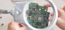
Read "chip packaging substrate"
3/9/2023 11:21:33 AM
• Packaging substrate occupies a key position in packaging materials, which puts forward higher requirements for packaging technology.
• Packaging substrate materials to high-end march, domestic enterprises in the core resin and photoresist and other fields have made breakthroughs.
• High-end copper foil and ceramic substrate are important areas in packaging substrate materials, and domestic enterprises are trying to catch up with international leaders.
First, the packaging substrate is the key to advanced packaging and domestic replacement, and the material industry chain is extended to the high-end
1. The packaging substrate accounts for the highest proportion of packaging materials and occupies a key position in flip packaging
Narrow packaging is mainly for first-level packaging, and packaging materials evolve to high standards. Semiconductor packaging is the last step in the semiconductor manufacturing process, providing electrical interconnection, mechanical support, mechanical and environmental protection and thermal conductivity channels between the chip and the printed circuit board.
The generalized package is mainly divided into zero-level to four-level package, zero-level package refers to the interconnection on the chip, the chip is obtained, the first-level package, that is, the narrow sense of the package, refers to the chip is fixed on the package substrate or lead frame, the chip pad and the package substrate or lead frame of the inner pin interconnection to further connect with the external pin, and the chip and the Internet for protective encapsulation.
The secondary package is board level package, that is, the printed circuit board is obtained. A tertiary/quaternary package will result in a complete electronic product. At present, integrated circuit chips are developing in the direction of large size, high integration, small feature size and high IO, so higher requirements are put forward for packaging technology, which is inseparable from the performance improvement and cost reduction of packaging materials. At present, packaging materials are developing in the direction of high thermal conductivity, high mechanical strength, high adhesion, low water absorption and low stress, promoting the continuous progress of advanced packaging.
Recommended News
-
Tel
+86-18718688232

 2023-03-09


